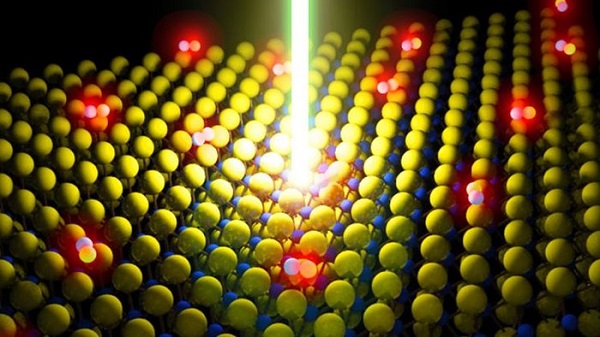
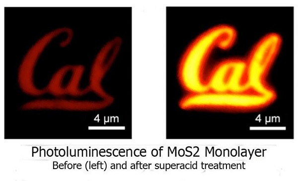
Engineers at the University of California at Berkeley and the Lawrence Berkeley National Laboratory have discovered a simple new process for repairing common defects on thin films. This discovery can promote the development of atomic single-layer semiconductors, suitable for transparent LED screens, high-efficiency solar cells, and micro-transistors. Treating a single-layer semiconductor made of molybdenum disulfide with super organic acids has enabled researchers to increase the efficiency of their materials by a factor of four. Lead researcher Ali Javey, a professor at the University of California, Berkeley, said: "This research is the first demonstration of 'a perfect single-layer photovoltaic material.' We have never heard of such a thin material before." The figure above shows a defect-free molybdenum disulfide (MoS2) monolayer semiconductor excited by a laser, which contributes to the development of transparent LED displays, ultra-efficient solar panels, photodetectors, and nano-sized transistors. The researchers created a layer of molybdenum disulfide only 7/10 nanometers thicker than human DNA 2.5 nm in diameter. Immersing the material in superacids removes contaminants and fills in missing atoms to repair defects - this chemical reaction is called protonation The industry’s strong interest in single-layer semiconductors stems from its low absorption of light and its ability to withstand twisting due to bending and other stresses. This makes it an ideal choice for transparent or flexible devices, such as deformable high-performance LED displays, and devices that can become transparent when the power is turned off. The left side of the figure above shows the MoS2 monolayer semiconductor in the shape of the Cal Logo; the right side of the figure above shows the effect after the super acid treatment. This process can also improve the performance of the transistor by removing defects. When the chip becomes smaller and thinner, the defect becomes an important obstacle to the development of the computer. Javey said: "The development of defect-free single-layer materials can also clear many of the problems encountered when developing new types of low-power switching devices." The team's work has been published in the recently published journal Science. Tea Strainer Silicone,Silicone Tea Strainer,Silicone Tea Bag Infuser,Silicone Tea Steeper YANGJIANG VOSSEN INDUSTRY AND TRADE CO.,LTD , https://www.cnvossen.com